
Jia Deng’s CAREER Award advances nano-manufacturing for the future of electronics
By Ethan Knox ’20 on JULY 07, 2025 @BingUNews
The first computers weighed over 30 tons and filled entire rooms. These days, they’re less than 20 pounds and can fit in backpacks. As technology continues to advance, electronics are getting even more compact. But this raises a fundamental question: How do we build on such a minuscule scale?
“In modern electronics, the brain of a cell phone is CPU circuits, or tiny transistors. How to manufacture technology as small as a thumbnail with billions of those transistors is a human industry miracle,” said Jia Deng, associate professor at the Thomas J. Watson College of Engineering and Applied Science’s School of Systems Science and Industrial Engineering. “But there is a need for individualized processes or for prototyping techniques. Probe-based nano-manufacturing would be more user-friendly, low cost and easy to handle, and has a lot of capability.”
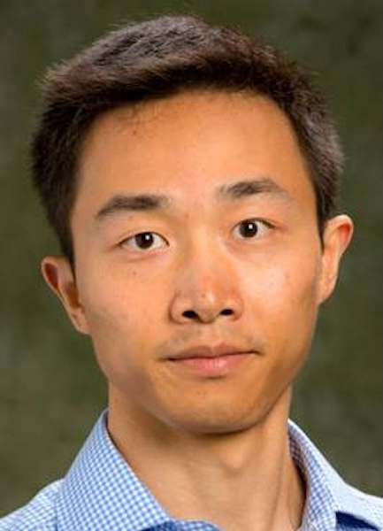
Deng joined SSIE as an assistant professor in 2017. He received a bachelor’s degree in process equipment and control engineering from the Wuhan University of Technology in 2010 and a master’s degree in mechatronics engineering from the Huazhong University of Science and Technology in 2013. His doctorate in industrial engineering was earned from North Carolina State University in 2017.
“I always felt manufacturing was something that enables and make things possible to realize. It supports and serves as the backbone to the industry,” Deng said. “You can design a rocket, but can you manufacture a rocket with available resources? Manufacturing for me was hands-on. I’d be able to create something useful.”
CAREER awards support research by early-career faculty who have the potential to serve as academic role models in research and education and to lead advances in the missions of their organizations.
To explore that topic, Deng recently received a prestigious NSF CAREER Award for his project “CAREER: Probe-Based Hybrid Nanopatterning of Conductive Polymers.” He has been awarded $580,623 to pursue this research.
Probe-based means that Deng is looking to investigate a manufacturing process that uses a tiny tool to interact with the materials. The project will use mechanical vibration and electric fields as hybrid energy forms to “mark” the target material. There are two potential ways the tool can use those energies to do this work — either by adding or removing material, or, more simply, making concave or convex features on the surface of the polymer.
This work with conductive polymers could significantly enhance the performance of nanoelectronics for a wide range of next-generation applications. However, nanopatterning of conductive polymers remains scientifically challenging, because these polymers are not compatible with existing patterning techniques.
The CAREER award supports fundamental research to address that knowledge gap. It is also expected to contribute to economic growth and national prosperity in the U.S. because of the booming electronic industry. It even supports educational programs to enhance engineering workforce training.
“This research will benefit our University and Watson, but even beyond that, we have outreach activities planned to engage local K-12 students. We hope to demonstrate various advanced manufacturing techniques,” Deng said. “This work can foster awareness and spark interest for local students in the engineering careers.”
The goals of the research are to investigate which properties and forms of the conductive materials affect the process most. Deng also hopes to develop a way to measure and assess the quality and reliability of nano-electronics made in this way.
Although this project is funded for only five years through the CAREER Award, Deng hopes the work extends far beyond that. In the future, he plans to experiment with other advanced materials that could advance the industry while continuing his personal scientific development.
“This process is robust and versatile. We’re also very interested in patterning two-dimensional materials that can be used for next generation devices, such as quantum devices,” Deng added. “In the next 10 to 30 years, I hope to become the top expert in the probe-based nano-manufacturing field and to establish national centers for nanomanufacturing and advanced nanoelectronics. I’d also like to work on translating manufacturing processes and findings from the lab to the production line and the industry level.”


Leave a comment